FPGA Architecture Basics
Table of Contents
This section is meant as a brief introduction to FPGA architecture and technology. Most people familiar with FPGAs can easily skip this section.
What is an FPGA?
An field programmable gate array (FPGA) is a special kind of chip (integrated circuit, silicon device, microchip, computer chip, or whatever designation is most familiar) that can be programmed to behave essentially like any other chip. One might think that a microprocessor or CPU falls into such a description as it is programmable through software compilation. However, an FPGA and CPU differ significantly in architecture and programming model.
CPU vs. FPGA
A central processing unit (CPU or just processor) follows the Von Neumann compute-based architecture as illustrated in the figure below.
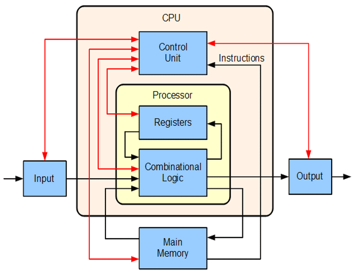
Basic Von Neumann Processing Model for CPUs (Source: Labtron, Creative Commons).
A control unit driven by instructions fetched from memory drives the flow of input data through the processor’s registers and logic producing outputs. The data paths, instruction set, register counts and memory interface are all fixed at the time of fabrication of the CPU. That is, they are unchanging attributes of the processor and cannot be customized later.
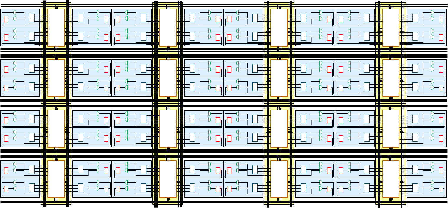
In stark contrast to the CPU architecture, an FPGA has highly configurable logic and data paths. This is enabled by a bit-wise, fine-grained architectural model to realize computation. In order to better understand how FPGAs work, it is beneficial to comprehend their atomic units of computation. Although modern FPGAs have a wide variety of components, at their heart is a large array of replicated programmable look-up tables (LUTs), flip-flops (or registers) and programmable wires called interconnect as seen in the figures below.
Hypothetical FPGA logic array of LUTs, flip flops and programmable wires (interconnect)
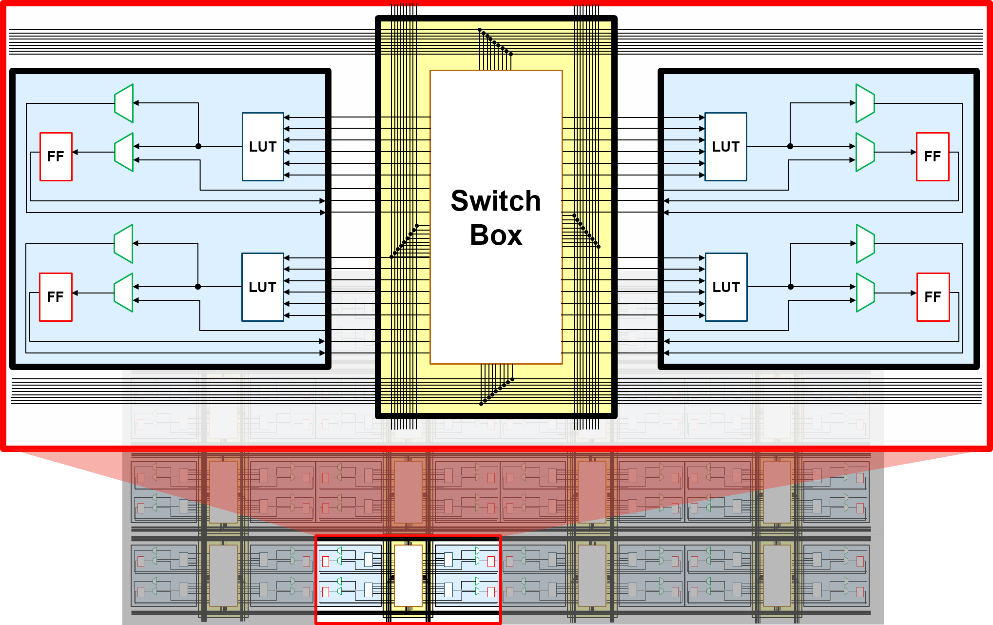
Close up view of replicated tiles of the logic array and interconnect
Lookup Tables (LUTs)
At the heart of configurable logic in FPGAs, lies a basic atomic unit of computation, a lookup table or LUT. A LUT has a single bit output that is calculated based on the input signal values and the configurable table (or memory) entries as shown in the figure below.
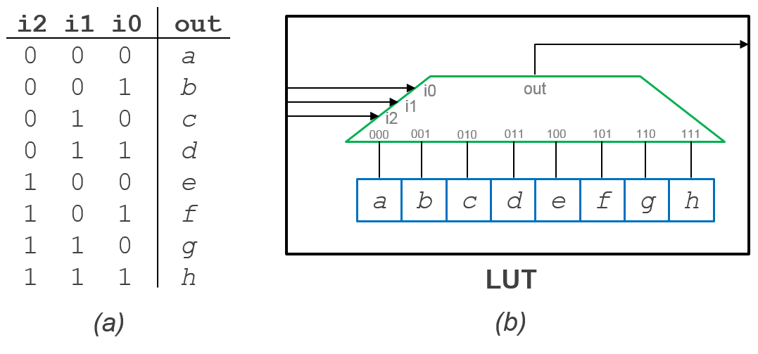
(a) Truth table relationship of a LUT (b) Diagram of logical behaviour of a LUT
Although mainstream FPGAs typically use 6-input LUTs, this example illustrates a 3-input LUT for simplicity but the principle of operation is the same.
LUTs are typically constructed using an N:1 multiplexer (shown in green in Figure 4b) and an Nx1-bit memory (shown in blue). The example in the figure above is a LUT where N=8. The number of inputs of a LUT is calculated as the log base 2 of N.
The memory entries in blue boxes in part (b) of the figure above represent the configurable table entries under the ‘out’ column in part (a). The vector of programming bits {a, b, … h} ultimately decide how the LUT will behave given different values presented on the inputs {i0, i1, i2}. For example, to program the LUT to evaluate “i0 XOR i1” on the inputs, the programming vector {a=0,b=1,c=1,d=0,e=0,f=1,g=1,h=0} would be used. A LUT can implement any Boolean logic equation limited only by the number of inputs of the LUT’s size. This characteristic is illustrated in the figure below. LUTs are commonly chained or combined in series to implement larger Boolean equations.
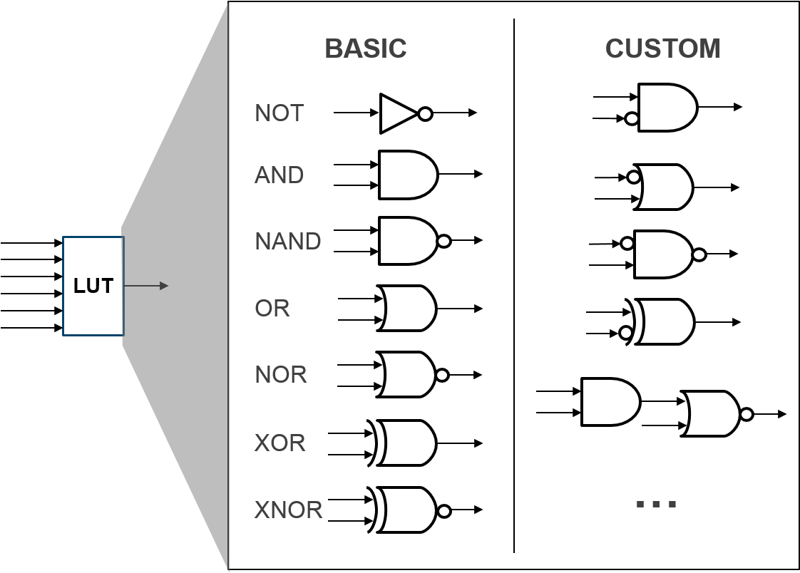
Examples of several (but not all) logic functions a LUT can potentially implement
In some devices, some of the LUTs have additional functionality then enable them to act as small RAMs. These RAMs can be chained together to build larger RAMs as well.
State Elements
Once a value is computed from a LUT, it often is desirable to store it. For this purpose, most FPGAs pair their LUTs with a D-flip-flop or equivalent state element. Often the storage element has configurable reset/clear and clock enable signals with an option of making it behave as a latch. These state elements have dedicated clocking paths to help minimize clock skew.
By chaining together LUTs and storing results in flip flops, FPGAs can implement any number of functions and computation limited only by the number of resources of the device and its delay.
Xilinx offers a variant of LUTs that enable them to also store data in the lookup portion of the table such that they can perform as small memories, shifters or FIFOs. More information on this can be found in Series 7 CLB User’s Guide or UltraScale CLB User’s Guide.
Carry Chains
Carry chain blocks are primitive elements that are provided with a group of LUTs to enable more efficient programmable arithmetic. Primarily it provides dedicated paths for the carry logic of simple arithmetic operations (add, subtract, comparisons, equals, etc). Implementing these arithmetic operations in LUTs would result in an inefficient use of resources and performance would suffer.
For more detailed information of Xilinx carry chains, please see Series 7 CLB User’s Guide or UltraScale CLB User’s Guide.
DSP Blocks
Multiplication on FPGAs can be quite expensive when implemented in LUTs and is a common operation. Therefore, dedicated hard blocks to provide integer multiplication have been present in FPGAs for several years. As applications have evolved, multiplier blocks have evolved to support a variety of DSP-friendly operations such as MAC (multiply, accumulate), wide AND/XOR and several others.
For more detailed information of Xilinx DSP blocks, please see Series 7 DSP User’s Guide or UltraScale DSP User’s Guide.
Block RAMs
Larger memories (than those made available as small LUTs) are also a significant resource on FPGAs that generally provide several kilobits of memory storage (Xilinx typically makes 18k or 36k available). These memories are provided in the fabric and are highly configurable and compose-able such that larger memories with several features can be made a available.
For more detailed information of Xilinx Block RAMs, please see Series 7 Memory User’s Guide or UltraScale Memory User’s Guide