Xilinx Architecture Terminology
Table of Contents
In order to use RapidWright, an understanding of Xilinx FPGA architecture and hierarchy will be necessary in navigating your way around the device APIs. In Xilinx FPGAs, there are six major levels of hierarchy that describe basic components all the way up to the entire device. This hierarchy can be seen in the figure below:
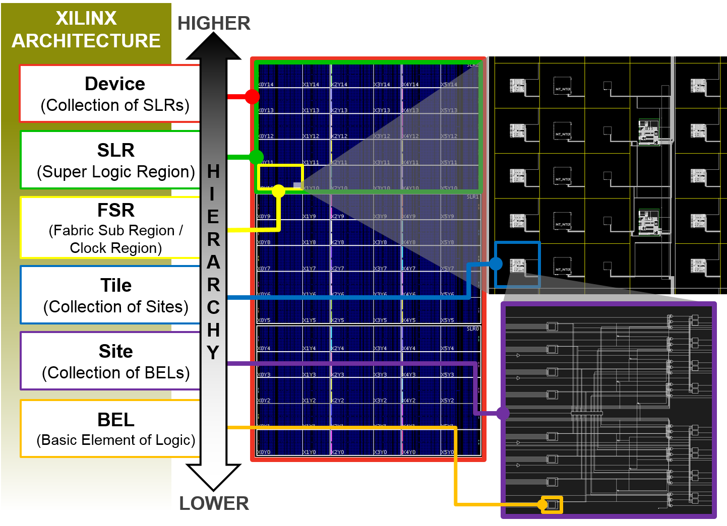
Levels of architectural hierarchy in Xilinx FPGAs.
We begin our discussion with a bottom-up approach starting with the lowest level of hierarchy, the basic element of logic.
BEL (Basic Element of Logic)
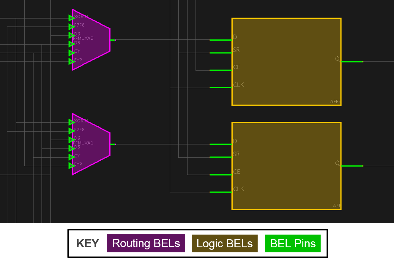
Vivado representation of two routing muxes (routing BELs) and two flip flops (logic BELs).
At the lowest level, the atomic unit of Xilinx FPGAs is a BEL. BELs are the smallest, indivisible, representable component in the fabric of an FPGA. There are two kinds of BELs, Logic BELs (Basic Element of Logic) and Routing BELs. A Logic BEL is a configurable logic-based site that can support the implementation of a design cell. Each BEL can support one or more types of UNISIM cells (UNISIM cells are described in Libraries Guides UG953 for Series 7 devices and UG974 for UltraScale™ devices). The mapping between a leaf cell (non-leaf cells do not represent implementable hardware, just hierarchy) in the netlist and a BEL site is referred to as the ‘placement’ of the cell. Thus, when one runs the Vivado command place_design, it is essentially mapping all leaf cells in the netlist to compatible and legal BEL sites.
Routing BELs are programmable routing muxes used to route signals between BELs. Routing BELs do not support any design elements (logic cells from the netlist do not occupy routing BEL sites), they are used only for routing. However, some routing BELs do have optional inversions.
BELs have input and output pins. BELs also have configurable connections that connect an input pin to an output pin. These BEL-based configurable connections are called site PIPs (where PIP stands for Programmable Interconnect Point). Both logic BELs and routing BELs can have site PIPs. However, in the case of a logic BEL, the site must be unoccupied by a cell in order for the route through to be usable. Often, these site PIPs, when implemented in logic BELs (a LUT is a common example), are referred to as a “route through” or “route-thru.” When routing a design, in order to physically route a net it is sometimes necessary to route through unused LUTs or other logic BELs with site PIPs.
Site
A group of related elements and their connectivity is referred to as a site. Inside of a site, one can find three major categories of objects:
BELs (Logic BELs and/or Routing BELs)
Site Pins (External input and output pins to the site)
Site wires (connecting elements to each other and site pins)
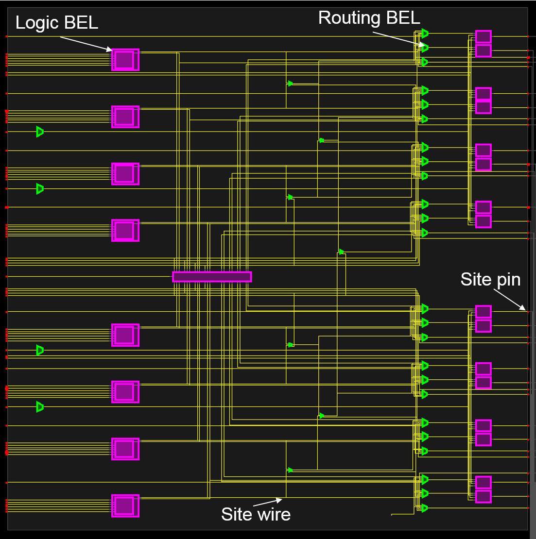
An UltraScale+ SLICEL site, where logic BELs are magenta, routing BELs are green, site pins are red and site wires are yellow.
Sites are instances of a type and each site has a unique name with an _X#Y# suffix denoting its location in the site type grid. Each site type will have its own XY coordinate grid, independent of others. The only exception to this is that SLICEL and SLICEM types share the same grid space. SLICEL and SLICEM are the most common site type and are the basic configurable logic building blocks that contain LUTs and flip flops that form the backbone of the FPGA fabric.
Site Type
Sites are heavily replicated across the device and each instance of a site corresponds to a site type of that device’s architecture family. Additionally, sites found in an FPGA device are sometimes capable of hosting different types, however, when a tile is queried, a ‘primary’ site type is designated.
Tile
At an abstract level, Xilinx devices are created by assembling a grid of tiles. Similar to sites, each tile is an instance of a type and each tile has a unique name with an _X#Y# suffix. Tiles are the building blocks used when constructing an FPGA device. Tiles are designed to abut one another when laid down to construct an FPGA device.
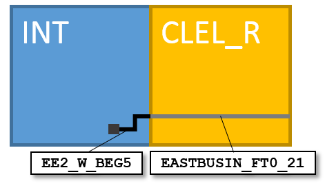
Not all tiles contain sites and those that do, can have more than one. Unlike sites and BELs, tiles do not have user visible pins. Instead, tiles contain uniquely-named wires that can connect to site pins or other wires through a programmable interconnect point (PIP). PIPs are programmable muxes that connect two wires together in the same tile. Most PIPs are present in switch box tiles (those with the “INT” prefix). Columns of switch box tiles are designed to connect to all fabric resources such as CLBs, DSPs, and BRAMs. When tiles abut, they are designed such that certain wires in the adjoining tiles line up and connect as shown in the figure below:
Node
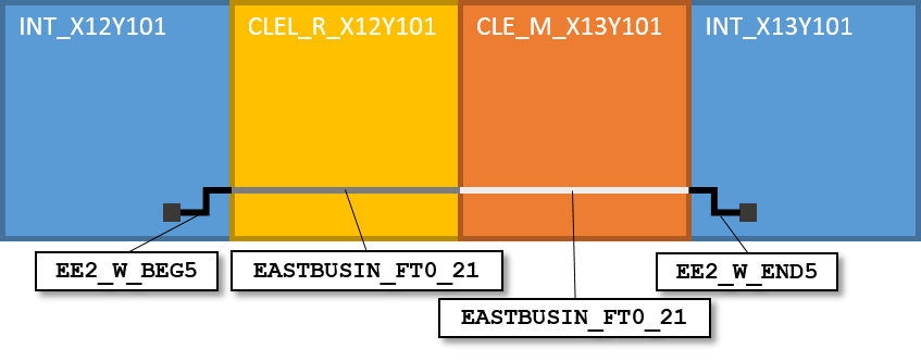
As there are no pins on tiles, the notion of a node is used to describe the connectivity of wires in between tiles. A node is a collection of electrically connected wires that spans one or more tiles. The figure below shows how four wires that abut among four tiles form a node:
Nodes and wires exist as first class Tcl objects in Vivado and the example above can be queried as follows:
% get_wires -of [get_node INT_X12Y101/EE2_W_BEG5]
INT_X12Y101/EE2_W_BEG5 INT_X13Y101/EE2_W_END5 CLEL_R_X12Y101/EASTBUSIN_FT0_21 CLE_M_X13Y101/EASTBUSIN_FT0_21
%
For additional resources regarding Vivado objects, see UG912: Vivado Design Suite Properties Reference Guide.
Tile Type
Each tile belongs to a type or definition. A tile type will contain the inventory list of all wires, PIPs and site types. Vivado does not directly represent the tile type as an object, but is listed as a property value under each tile.
Xilinx traditionally has leveraged a columnar-based architectural approach to tile layout. That is, with a few exceptions, all tiles within a column are of the same type but tiles occupying the same row are typically different types.
FSR (Fabric Sub Region or Clock Region)
A fabric sub region, also known as a clock region, is a replicated 2D array of tiles in the fabric. In the UltraScale architecture, all FSRs are 60 CLBs tall, but their width will vary depending on the mix of tile types used in its construction.
Clock routing and distribution lines are represented as the same granularity as FSRs. In UltraScale architectures, there are 24 horizontal routing tracks, 24 vertical routing tracks, 24 horizontal distribution tracks and 24 vertical distribution tracks. These routing and distribution tracks abut to tracks in neighboring FSRs to form the device clock network resource set. For more information specific to clocking resources, please see UG472: Series 7 Clocking Resources User Guide or UG572: UltraScale Architecture Clocking Resources User Guide.
SLR (Super Logic Region)
This level of hierarchy is only present on devices that use the stacked silicon interconnect technology (SSIT) or also known as 2.5D packaging using a silicon interposer. As multiple dies (or dice) are packaged together, each die becomes a super logic region or SLR. SLRs contain a 2D array of FSRs and are typically identical as each die is fabricated from the same mask set.
In order for logic to communicate between SLRs, the UltraScale architecture employ special tiles in the FSRs neighbouring the abutment of two SLRs. A column of CLBs is removed and replaced with special tiles called Laguna tiles that have dedicated flip flop sites to aid in crossing the SLR divide.
